IS2.2 Atomic level control & nanostructuring
Infrastructure:
Laser plasma setup for thin DLC layers, Low contamination prototyping, 3D printing
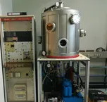
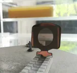
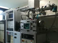
A key infrastructure in the development of new experimental techniques is the ability to provide on demand surface coatings and thin films on a short time scale. The thin-film lab supports very different tasks ranging from surface coatings for optical or UV mirrors, photosensitive cathode materials to complex multilayer structures for neutron detection. For vapor deposition, we apply different methods like Joule heating, electron beam heating or laser plasma deposition. Our workhorse is a 60 cm Varian 3119 R&D coater system (see fig. 1) with a 10 kW electron gun. A special laser plasma deposition plant (see fig. 2) with a Spectron Laser SL801 (0.4 J pulse energy) allows for the production of ultra-thin (1 - 15 µg/cm2) self-supporting diamond like carbon (DLC) foils. These foils can be produced up to a maximum diameter of 200 mm (see fig. 3).
Typical applications: secondary electrons, charge stripping, detector windows, particle accelerators, particle detector development, optical coatings, photo cathodes, monoisotopic targets
| Principal investigator | Prof. Dr. Laura Fabbietti |
| PI's field of research | Particle & nuclear physics |
| Contact person | Dr. Roman Gernhäuser |
| Tel. | +49 89 289 12440 |
| roman.gernhaeuser@ph.tum.de | |
| Availability | cooperation & pay-by-use |
| Lead time | depends on application (one week - six months) |
Laser Induced Current Transient technique which enables detailed investigation of electrified interfaces. Pulsed laser technique coupled with potentiostat and quartz crystal microbalance.
Typical applications: electrocatalysis, solid/liquid interfaces of functional materials
| Principal investigator | Prof. Dr. Aliaksandr Bandarenka |
| PI's field of research | Energy conversion and storage materials |
| Contact person | Theophilus Kobina Sarpey |
| Tel. | +49 89 289 12540 |
| theok.sarpey@tum.de | |
| Availability | cooperation |
| Lead time | within weeks of contacting; typical measurements can be done within a day |
High-end mid-IR FTIR spectrometer (resolution 0.2 cm-1) with sample holders to work in transmission and ATR configuration, rapid scan option, polarization modulation and 2D FT-IR mapping capabilities
Typical applications: identification of both organic and inorganic compounds and the detection of adsorbates and intermediates at electrochemical interfaces.
| Principal investigator | Prof. Dr. Katharina Krischer |
| PI's field of research | Self-Organization at Interfaces, Artificial Photosynthesis, Electrocatalysis |
| Contact person | Simon Stork |
| Tel. | +49 89 289 13877 |
| simon.stork@tum.de | |
| Availability | cooperation & pay-by-use |
| Lead time | depending on application |
Cleanroom for standard optical lithography
Available equipment: wet benches, fume hoods, optical lithography, standard thin film materials by thermal evaporation for contacts etc., atomic layer deposition for AlOx, critical point dryer, wire and ball bonder etc.
Typical applications: Nanostructuring of spintronics materials
| Principal investigator | Prof. Dr. Christian Back |
| PI's field of research | Magnetism, Spintronics, Magnetic materials |
| Contact person | Dr. Thomas Meier |
| Tel. | +49 89 289 12403 |
| thomas2.meier@tum.de | |
| Availability | cooperation |
| Lead time | no lead time for standard processes |